The LSI-11 is the low-end member of DIGITAL's bus family. All DIGITAL microcomputers use the LSI-11 Bus. Originally 16-bit data and addressing, it has been extended to accomodate 18 and 22 bit addressing.
The bus consists of 42 bidirectional and 2 unidirectional signal lines as follows:-
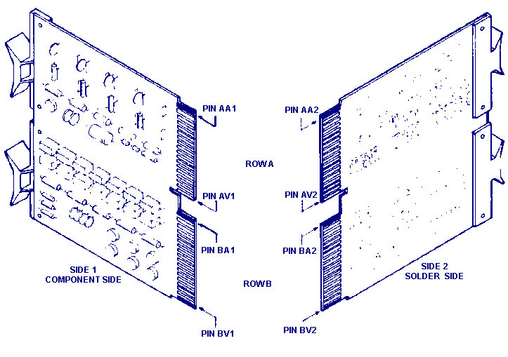
The backplane consists of rows of bus connectors, each of which have four slots (labelled A, B, C, D). Each slot accomodates 36 connectors, 18 on the component side of the board and 18 on the solder side. Physically, this is the same format as the PDP-8 UNIBUS.
An individual finger on a circuit board or connector in the backplane can thus be identified uniquely. For example:-
                        BE2  SLOT B
                             Finger/Connector E
                             Solder side (2)
| BUS PIN |
MNEMONIC | FUNCTION | DESCRIPTION |
|---|---|---|---|
| AA1 | BIRQ5 L | Interrupt Control |
Interrupt Request Priority Level 5 |
| AB1 | BIRQ6 L | Interrupt Control |
Interrupt Request Priority Level 6 |
| AC1 | BDAL16 L | Data/Address | Extended address bit during addressing protocol; memory error data line during data transfer protocol. |
| AD1 | BDAL17 L | Data/Address | Extended address bit during addressing protocol; memory error logic enable during data transfer protocol. |
| AE1 | SSPARE1 (Alternate +5B) |
Spare | Special Spare: Not assigned or bused in DIGITAL cable or backplane assemblies; available for user connection. Optionally, this pin may be used for +5V battery (+5B) backup power to keep critical circuits alive during power failures. A jumper is required on LSI-11 Bus options to open (disconnect) the +5B circuit in systems that use this line as SSPARE1. |
| AF1 | SSPARE2 | Spare | Special Spare—not assigned or bused in DIGITAL cable or backplane assemblies; available for user interconnection. In the highest-priority device slot, the processor may use this pin for a signal to indicate its RUN state. |
| AH1 | SSPARE 3 SRUN simultaneously |
Spare | Special Spare— not assigned or bused in DIGITAL cable or backplane assemblies; available for user interconnection. An alternate SRUN signal may be connected in the highest-priority set. |
| AJ1 | GND | Power and ground |
Ground— System signal ground and dc return. |
| AK1 | MSPAREA | Spare | Maintenance Spare— Normally connected together on the backplane at each option location (not bused connection). |
| ALl | MSPAREB | Spare | Maintenance Spare— Normally connected together on the backplane at each option location (not bused connection). |
| AM1 | GND | Power and ground |
Ground— System signal ground and dc return. |
| AN1 | BDMR L | DMA Control |
Direct Memory Access (DMA) Request— A device asserts this signal to request bus mastership. The processor arbitrates bus mastership between itself and all DMA devices on the bus. If the processor is not bus master (it has completed a bus cycle and BSYNC L is not being asserted by the processor), it grants bus mastership to the requesting device by asserting BDMGO L. The device responds by negating BDMR L and asserting BSACK L. |
| AP1 | BHALT L | System Control |
Processor Halt— When BHALT L is asserted for at least 25 µs, the processor services the halt interrupt and responds by halting normal program execution. External interrupts are ignored but memory refresh interrupts in LSI-11 are enabled if W4 on M7264 and M7264-YA processor modules is removed and DMA request/grant sequences are enabled. The processor executes the ODT microcode and the console device operation is invoked. |
| AR1 | BREF L | System Control |
Memory Refresh— Asserted by a DMA device. This signal forces all dynamic MOS memory units requiring bus refresh signals to be activated for each BSYNC L/BDIN L bus transaction. It is also used as a control signal for block mode DMA. CAUTION The user must avoid multiple DMA data transfers (burst or "hog" mode) that could delay refresh operation if using DMA refresh. Complete refresh cycles must occur once every 1.6 msec if required. |
| ASl | +12B or +5B |
Power and ground |
+12 Vdc or +5V battery or backup power to keep critical +5B circuits alive during power failures. This signal is not bused to BSl in all DIGITAL backplanes. A jumper is required on all LSI-11 Bus options to open (disconnect) the backup circuit from the bus in systems that use this line at the alternate voltage. |
| AT1 | GND | Power and ground |
Ground— System signal ground and dc return. |
| AU1 | PSPARE 1 | Spare | Spare (Not assigned. Customer usage not recommended.) Prevents damage when modules are inserted upside down. |
| AV1 | +5B | Power and ground |
+5V Battery Power— Secondary +5V power connection. Battery power can be used with certain devices. |
| BA1 | BDCOK H | System Control |
DC Power OK— Power supply. generated signal that is asserted when there is sufficient dc voltage available to sustain reliable system operation. |
| BB1 | BPOK H | System Control |
Power OK— Asserted by the power supply 70 ms after BDCOK negated when ac power drop below the value required to sustain power (approximately 75% of nominal). When negated during processor operation, a power fail trap sequence is initiated. |
| BC1 | SSPARE4 BDAL 19L (22-bit only) |
Data/Address | Special Spare in the LSI-11 Bus— Not assigned. Bussed in 22-bit cable and backplane assemblies; available for user interconnection. |
| BD1 | SSPARE5 BDAL 19L (22-bit only) |
Data/Address | Caution. These pins may be used as test points by DIGITAL in some options. |
| BE1 | SSPARE6 BDAL 20L |
Data/Address | In the 22-bit LSI-11 Bus, these bussed address lines are Address Lines <21:18> currently not used during data time. |
| BF1 | SSPARE7 BDAL 21L |
Data/Address | In the 22-bit LSI-11 Bus these bussed address lines are Address Lines <21:18> currently not used during data time. |
| BH1 | SSPARE8 | Spare | Special Spare— Not assigned or bused in DIGITAL cable and backplane assemblies; available for user interconnection. |
| BJ1 | GND | Power and Ground |
Ground— System signal ground and dc return. |
| BK1 BL1 |
MSPAREB MSSPAREB |
Spare | Maintenance Spare— Normally connected together on the backplane at each option location (not a bused connection). |
| BM1 | GND | Power and Ground |
Ground— System signal ground and dc return. |
| BN1 | BSACK L | DMA Control |
This signal is asserted by a DMA device in response to the processor's BDMGO L signal, indicating that the DMA device is bus master. |
| BP1 | BIRQ7 L | Interrupt Control |
Interrupt request priority level 7 |
| BR1 | BEVNT L | System Control |
External Event Interrupt Request— When asserted, the processor responds by entering a service routine via vector address 1OO8. A typical use of this signal is a line time clock interrupt. |
| BS1 | +12B | Power and Ground | +12 Vdc battery backup power (not bused to AS1 in all DIGITAL backplanes). |
| BT1 | GND | Power and Ground |
Ground— System signal ground and dc return. |
| BU1 | PSPARE2 | Spare | Power Spare 2 (not assigned a function, not recommended for use). If a module is using -12V (on pin AB2) and if the module is accidentally inserted upside down in the backplane, -12 Vdc appears on pin BU1. |
| BV1 | +5 | Power and Ground |
+5V Power— Normal +5 Vdc system power. |
| AA2 | +5 | Power and Ground | +5V Power— Normal +5 Vdc system power. |
| AB2 | -12 | Power and Ground |
-12VPower— -12Vdc(optional) power for devices requiring this voltage. NOTE LSI-11 modules which require negative voltages contain an inverter circuit (on each module) which generates the required voltage(s). Hence, -12V power is not required with DIGITAL-supplied options. |
| AC2 | GND | Power and Ground |
Ground— System signal ground and dc return. |
| AD2 | +12 | Power and Ground |
+12V Power— +12 Vdc system power. |
| AE2 | BDOUT L | Data Control |
Data Output— BDOUT, when asserted, implies that valid data is available on BDAL <0:15> L and that an output transfer, with respect to the bus master device, is taking place. BDOUT L is deskewed with respect to data on the bus. The slave device responding to the BDOUT L signal must assert BRPLY L to complete the transfer. |
| AF2 | BRPLY L | Data Control |
Reply— BRPLY L is asserted in response to BDIN L or BDOUT L and during IAK transactions. It is generated by a slave device to indicate that it has placed its data on the BDAL bus or that it has accepted output data from the bus. |
| AH2 | BDIN L | Data Control | Data Input— BDIN L is used for two types of bus operation: When asserted during BSYNC L time, BDIN L implies an input transfer with respect to the current bus master, and requires a response (BRPLY L). BDIN L is asserted when the master device is ready to accept data from a slave device. When asserted without BSYNC L, it indicates that an interrrupt operation is occurring. The master device must deskew input data from BRPLY L. |
| AJ2 | BSYNC L | Data Control |
Synchronize— BSYNC L is asserted by the bus master device to indicate that it has placed an address on BDAL.<0:17> L. The transfer is in process until BSYNC L is negated. |
| AK2 | BWTBT L | Data Control |
Write/Byte— BWTBT L is used in two ways to control a bus cycle: It is asserted at the leading edge of BSYNC L to indicate that an output sequence is to follow (DATO or DATOB), rather than an input sequence. It is asserted during BDOUT L, in a DATOB bus cycle, for byte addressing. |
| AL2 | BIRQ4 L | Interrupt Control |
Interrupt Request Priority Level 4— A level 4 device asserts this signal when its interrupt enable and interrupt request flips-flops are set. If the PS word bit 7 is 0, the processor responds by acknowledging the request by asserting BDIN L and BIAKO L. |
| AM2 AN2 |
BIAKI L BIAKO |
Interrupt Control |
Interrupt Acknowledge— In accordance with interrupt protocol, the processor asserts BIAKO L to acknowledge receipt of an interrupt. The bus transmits this to BIAKI L of the device electrically closest to the processor. This device accepts the interrupt acknowledge under two conditions: 1) The device requested the bus by asserting BIRQXL, and 2) the device has the highest-priority interrupt request on the bus at that time. If these conditions are not met, the device asserts BIAKO L to the next device on the bus. This process continues in a daisy-chain fashion until the device with the highest-interrupt priority receives the interrupt acknowledge signal. |
| AP2 | BBS7 L | Data Control |
Bank 7 Select— The bus master asserts this signal to reference the I/O page (including that portion of the I/O page reserved for nonexistent memory). The address in BDAL<0:12> L when BBS7 L is asserted is the address within the I/O page. |
| AR2 AS2 |
BDMGI L BDMGO L |
DMA Control |
Direct Memory Access Grant— The bus
arbitrator asserts this signal to grant bus mastership to a
requesting device, according to bus mastership protocol. The
signal is passed in a daisy-chain from the arbitrator (as BDMGO
L) through the bus to BDMGI L of the next priority device
(electrically closest device on the bus). This device accepts the
grant only if it requested to be bus master (by a BDMR L). If
not, the device passes the grant (asserts BDMGO L) to the next
device on the bus. This process continues until the requesting
device acknowledges the grant. CAUTION DMA device transfers must not interfere with the memory refresh cycle. |
| AT2 | BINIT L | System Control |
Initialize— This signal is used for system reset. All devices on the bus are to return to a known, initial state; i.e., registers are reset to zero, and logic is reset to state 0. Exceptions should be completely documented in programing and engineering specifications for the device. |
| AU2 AV2 |
BDAL0 L BDAL1 l |
Data/Address | Data/Address lines— These two lines are part of the 16-line data/address bus over which address and data information are communicated. Address information is first placed on the bus by the bus master device. The same device then either receives input data from, or outputs data to the addressed slave device or memory over the same bus lines. |
| BA2 | +5 | Power and Ground | +5V Power— Normal +5 Vdc system power. |
| BB2 | -12 | Power and Ground | -12V Power—- -12Vdc(optional) power
for devices requiring this voltage. (Voltage normally not supplied by DIGITAL). |
| BC2 | GND | Power and Ground | Ground— System signal ground and dc return. |
| BD2 | +12 | Power and Ground | +12V Power— +12Vsystem power. |
| BE2 | BDAL2 L | Data/Address | Data/Address Lines— These 14 lines are part of the 16-line data/address bus previously described. |
| BF2 | BDAL3 L | ||
| BH2 | BDAL4 L | ||
| BJ2 | BDAL5 L | ||
| BK2 | BDAL6 L | ||
| BL2 | BDAL7 L | ||
| BM2 | BDAL8 L | ||
| BN2 | BDAL9 L | ||
| BP2 | BDAL10 L | ||
| BR2 | BDAL11 L | ||
| BS2 | BDAL12 L | ||
| BT2 | BDAL13 L | ||
| BU2 | BDAL14 L | ||
| BV2 | BDAL15 L |